

Elon Musk’s Terafab: A Comprehensive Review of the New AI Chip Megaproject
Terafab is Elon Musk’s proposed attempt to build a semiconductor manufacturing system on a scale intended to serve Tesla, SpaceX and xAI. It is not simply another Tesla factory. The project aims to combine chip design, advanced logic fabrication, memory production, photomasks, packaging and testing within a vertically integrated operation capable of supporting autonomous vehicles, humanoid robots, large AI models and, eventually, computing infrastructure in space.
The ambition is extraordinary: Musk has described a long-term target of producing one terawatt of computing capacity each year. That figure is a statement of intended compute output, not the electrical consumption of one completed building, and it should not be confused with current production. As of October 2026, Terafab is a developing programme consisting of announced plans, recruitment, a smaller research-fab strategy, proposed large-scale construction in Texas and negotiations across a complex semiconductor supply chain.
This review separates what has been confirmed from what remains a target. It examines the project’s origins, locations, manufacturing model, Intel relationship, expected products, economics, energy and water requirements, strategic value, risks and realistic prospects.

What Terafab Is
Terafab is a planned advanced-semiconductor programme associated with Tesla, SpaceX and SpaceX’s xAI business. Its defining feature is vertical integration. Instead of designing chips and sending every manufacturing stage to separate suppliers around the world, the project aims to bring logic, memory, advanced packaging, testing and lithography-mask capability into a closely connected manufacturing system.
Tesla’s own recruitment material describes Terafab as a vertically integrated semiconductor factory operating at unprecedented scale. Vacancies have appeared for specialists in logic and memory devices, dry etch, process integration, thin-film materials, module processing and mechanical tooling. Recruitment does not prove that the final megafab has been built, but it is concrete evidence that engineering teams are being assembled.
The name follows Musk’s established progression from Gigafactory to Terafab. In semiconductor terms, however, scale cannot be increased as simply as factory floor area. A leading-edge fab requires extreme process control, thousands of specialised tools, mature recipes, highly trained staff, dependable utilities and years of yield improvement.
Why Musk Says It Is Necessary
Tesla needs custom inference processors for vehicles, robotaxis and Optimus robots. xAI needs enormous quantities of high-performance accelerators and memory for training and operating AI models. SpaceX is exploring processors designed for satellites and proposed orbital computing infrastructure. Musk argues that even aggressive supply projections from existing manufacturers will not cover the combined future demand of these businesses.
This is the central strategic case for Terafab: semiconductor supply has become a constraint on Musk’s broader plans. Building an internal capability could provide priority access to chips, tighter hardware-software co-design and faster experimentation. It could also reduce exposure to overseas concentration, particularly the dependence of leading-edge fabrication on Taiwan and South Korea.
The counterargument is equally important. TSMC, Samsung, Intel, Micron and their equipment partners have accumulated decades of manufacturing knowledge. Creating capacity is difficult; producing competitive chips reliably and economically is harder. Terafab would still depend on external suppliers for lithography systems, deposition and etch equipment, materials, chemicals, substrates and many other inputs.
The Companies Involved
Tesla contributes automotive and robotics chip design, high-volume manufacturing experience and the immediate requirement for efficient edge inference. Its vehicles and Optimus robots need processors that deliver high performance within strict power, thermal, safety and cost limits.
SpaceX is expected to lead important parts of the larger industrial development. Its interests include satellite electronics, launch systems and the much more speculative concept of placing large-scale AI compute in orbit. SpaceX also has experience rapidly expanding complex hardware production, although semiconductor fabrication is a very different discipline.
xAI provides the demand for training and inference compute. Large AI clusters consume accelerators, networking components and high-bandwidth memory at extraordinary rates. Terafab could eventually give xAI access to processors designed around its own models rather than relying almost entirely on merchant GPUs.
Intel has been identified as a technology and manufacturing partner, with Musk stating that Terafab plans to use Intel’s 14A process. Intel’s participation could supply essential process knowledge and a route to advanced manufacturing technology. The exact commercial, licensing and operational arrangements remain critical unknowns.
Two Development Tracks: Research Fab and Full-Scale Complex
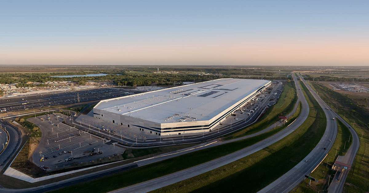
The project is best understood as two related tracks rather than one instantly completed factory. Tesla has discussed a smaller research fab at or near Giga Texas in Austin. Musk described this facility as capable of producing perhaps a few thousand wafers per month and intended primarily to test ideas, revise designs and accelerate learning.
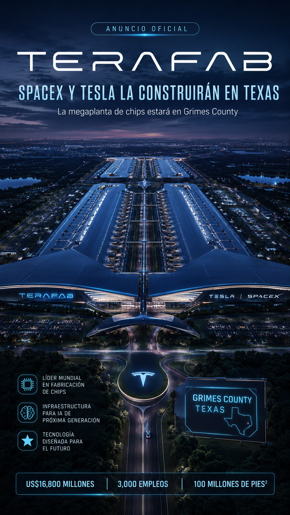
The proposed full-scale facility is associated with Grimes County, Texas. Public reporting has described a much larger SpaceX-led semiconductor complex and potential investment rising dramatically if all phases proceed. Figures quoted for early and total investment vary because they refer to different filings, stages and scenarios. They should not be treated as one guaranteed budget.
The research fab makes strategic sense even if the megaproject changes. A pilot line can help engineers understand manufacturability, test new packaging and memory combinations, train staff and shorten the feedback loop between chip design and physical silicon. It cannot, by itself, produce the volumes implied by the full Terafab vision.
What Would Be Manufactured?
The expected product mix spans several very different workloads. Tesla’s next-generation AI chips are intended for real-time perception and decision-making in vehicles and robots. These processors must balance compute performance against power use, heat, latency, physical size, automotive qualification and cost.
xAI’s data-centre requirements are different. Training frontier models demands dense arithmetic performance, very high memory bandwidth, fast interconnects and large packaging systems that combine multiple dies. Space-based processors would add radiation tolerance, severe thermal constraints, launch mass and long-term reliability.
A single process cannot necessarily optimise every product. Terafab may need multiple process technologies, specialised packaging and different qualification regimes. The value of integration would come from coordinating these elements—not from forcing every chip through one identical production flow.
Logic, Memory and Advanced Packaging Under One Roof
Traditional semiconductor supply chains are highly specialised. One company may design a processor, another manufacture its logic dies, another supply memory, and an outsourced assembly-and-test provider package the components. Terafab proposes to place more of that chain under common control.
Logic fabrication creates the computational parts of a chip. Memory production supplies the capacity and bandwidth needed to keep processors fed with data. Advanced packaging connects multiple logic and memory dies with extremely high-speed links. Testing identifies failures and verifies that completed devices meet performance and reliability requirements.
Bringing these stages closer together could speed iteration and allow chips, memory and packaging to be designed as one system. It also multiplies the execution challenge. Logic, DRAM-class memory, packaging and mask production are each difficult industries with different equipment, expertise and economics.
Intel 14A and the Manufacturing Technology
Intel 14A is a future-generation process platform rather than a mature commodity production line. Musk has said Terafab intends to use it once the process is ready for prime time. For Intel, a successful Terafab commitment could provide a major customer and validation for its foundry strategy. For Musk’s companies, Intel could provide a domestic advanced-node route and knowledge that cannot be recreated quickly.
The risk is schedule coupling. If 14A development, equipment installation or yield improvement is delayed, Terafab products could also be delayed. Conversely, designing chips for an immature process creates uncertainty around performance, power, area, defect rates and cost.
Even a strong process design kit does not create a production-ready fab. Each tool must be installed, calibrated and integrated into a process containing hundreds or thousands of steps. Yield—the proportion of usable chips produced from each wafer—determines whether technically working silicon can become economically viable.

Understanding the One-Terawatt Target
The one-terawatt figure is easy to misunderstand. Terafab’s stated ambition concerns annual production of chips representing roughly one terawatt of compute power when deployed. It does not mean a completed Terafab building is currently drawing one terawatt from the Texas grid.
There is no universal conversion between watts and numbers of chips because devices differ in performance and power. One terawatt could represent billions of low-power edge processors, millions of high-power accelerators or a mixture of products. Packaging, memory and system overhead further complicate any comparison.
The target is therefore best read as a declaration of desired industrial scale, not a precise forecast of finished annual output. Reuters reported that analysts considered the capital needed to support a full terawatt of advanced compute to be measured in trillions of dollars if interpreted across the complete required manufacturing capacity. That gap shows how far the long-term vision extends beyond the presently identified phases.
Reality check: Terafab is an active project, but it is not yet a completed one-terawatt fab. The most defensible current description is a staged semiconductor initiative with a research-fab plan, a proposed Texas megasite, active recruitment, stated Intel 14A intentions and exceptionally ambitious long-term production targets.
Location, Jobs and Regional Impact
Austin is the centre of the early research effort and already hosts Tesla’s headquarters and Giga Texas. The larger proposed development has been linked to Grimes County, northwest of Houston and southeast of College Station. The region offers land, access to infrastructure and proximity to Texas’s expanding semiconductor and technology ecosystem.
A project of this scale could create thousands of direct jobs and many more construction, logistics and supplier positions. High-value roles would include device engineering, process integration, equipment maintenance, facilities engineering, materials science, contamination control, packaging, testing and factory software.
The local effects would not all be positive. Large construction programmes can strain roads, housing, emergency services and local labour markets. Long-term tax incentives need to be weighed against public infrastructure demands and the risk that later phases are reduced or delayed.
Power, Water and Environmental Pressure
Semiconductor fabs require exceptionally reliable electricity. Brief interruptions or voltage instability can damage work in progress and disrupt equipment. Terafab would need substantial generation, transmission, backup and power-conditioning infrastructure, especially if logic, memory and packaging operate on the same campus.
Water is equally important. Chip production uses ultra-pure water for repeated cleaning stages. Public plans have discussed reservoir water, treatment and recycling rather than relying entirely on local groundwater, but the final demand will depend on the number of production lines, process nodes and recycling efficiency.
The environmental assessment must include more than headline water consumption. Fabs use industrial gases, solvents, acids and other chemicals; they produce wastewater and greenhouse-gas emissions; and their equipment and buildings embody enormous material and energy costs. Effective containment, abatement, recycling and transparent monitoring would be essential.
Supply-Chain Independence—But Not Total Independence
Terafab could reduce dependence on external wafer capacity, but it cannot create a self-contained semiconductor civilisation. Leading-edge lithography depends heavily on ASML. Deposition, etch, inspection and metrology rely on companies such as Applied Materials, Lam Research, Tokyo Electron and KLA. Materials and components come from a global network of specialist suppliers.
True resilience comes from multiple qualified sources, inventory planning, maintainable equipment and realistic geographic diversification. Replacing reliance on one foundry with reliance on one internal campus would create a different concentration risk.
The strongest strategic outcome may be a hybrid model: Terafab supplies proprietary or strategically critical devices while TSMC, Samsung, Intel and others continue to provide additional capacity and process options.
The Potential Advantages
- Hardware-software co-design: chips can be tailored closely to Tesla autonomy, Optimus, xAI models and SpaceX systems.
- Faster iteration: a nearby research fab can shorten the cycle between design, fabrication, testing and redesign.
- Priority capacity: internal production could reduce competition for limited external advanced-node supply.
- Packaging integration: logic, memory and interconnect can be developed as a complete computing system.
- Domestic capability: Texas-based production could diversify advanced semiconductor manufacturing geographically.
- Scale economics: if demand and yield are both achieved, very high internal consumption could support dedicated production.
The Main Risks
Execution risk is the largest issue. Semiconductor manufacturing punishes shortcuts. New buildings, tools, recipes, staff and supply chains must operate together with microscopic precision. A factory can be physically complete while commercially useful output remains low.
Financial risk is substantial. Initial phases may cost tens of billions of dollars, while the complete one-terawatt vision implies far more. Tesla, SpaceX and xAI are simultaneously funding vehicles, robots, rockets, satellites, data centres, energy infrastructure and AI development.
Technology risk includes process delays, poor yield, packaging bottlenecks and rapidly changing AI architectures. A facility optimised for one design approach could need expensive changes if model architectures or memory technologies shift.
Demand risk also matters. The business case assumes enormous adoption of autonomous vehicles, Optimus robots, xAI services and space-based computing. If those markets grow more slowly than expected, internal demand may not justify all proposed capacity.
Governance risk arises from several Musk-controlled businesses sharing investment, technology and output. Investors and regulators will want clarity about ownership, pricing, intellectual property, liabilities and which company carries the cost of each phase.
How Terafab Compares with Established Fabs
TSMC leads the pure-play foundry model, manufacturing advanced chips designed by many customers. Samsung combines foundry, memory and device businesses. Intel manufactures its own processors while attempting to expand as a contract foundry. Terafab is different because it is conceived primarily around the future internal needs of a connected group of companies.
Its proposed combination of logic, memory and packaging is strategically attractive, but established manufacturers already pursue advanced packaging and system-level integration. Terafab’s distinguishing claim is the degree of common ownership, customisation and scale—not the invention of every underlying manufacturing method.
The correct benchmark will not be the size of the building or the number announced on stage. It will be qualified wafers, usable packaged systems, yield, cost, energy efficiency, reliability and on-time delivery.
Could Terafab Enable AI in Space?
Space-based data centres are among the project’s most futuristic justifications. Orbit offers access to solar energy and, in some configurations, radiative cooling. Starship could reduce launch costs sufficiently to make much larger orbital systems conceivable.
The difficulties are formidable. High-performance processors generate intense heat, and vacuum prevents ordinary convective cooling. Large radiators add mass and area. Radiation damages electronics. Hardware repairs and upgrades are difficult. Data must move between Earth and orbit, adding networking constraints and requiring large communications systems.
Terafab could produce specialised space processors whether or not orbital AI data centres become economical. Radiation-tolerant, power-efficient chips for satellites represent a more immediate and credible market than replacing terrestrial AI campuses at scale.
What Success Would Look Like
The first credible sign of success would be a functioning research line producing repeatable test wafers and useful prototype devices. The next would be qualified products with improving yield, followed by dependable volume output for Tesla, SpaceX or xAI.
Construction announcements and equipment orders are necessary milestones, but not proof of semiconductor success. Investors and observers should look for measurable indicators:
- Completed cleanroom and utility infrastructure.
- Installed and qualified manufacturing tools.
- First silicon and independently verifiable product demonstrations.
- Yield improvement across successive production runs.
- Automotive, data-centre or space qualification.
- Packaged chips deployed in commercial products.
- Transparent capital spending, ownership and production schedules.
Overall Assessment
Terafab addresses a genuine strategic issue: advanced AI ambitions increasingly depend on access to specialised chips, memory and packaging. Tesla, SpaceX and xAI have enough combined demand to justify deeper involvement in semiconductor design and production. A focused research fab and selective internal manufacturing could deliver valuable results even if the largest claims are never reached.
The full vision is much less certain. Producing one terawatt of annual compute would require capital, equipment, utilities, materials and skilled labour on a scale far beyond an ordinary factory expansion. The project must master several manufacturing disciplines simultaneously while Intel’s proposed 14A technology is itself still developing.
The sensible conclusion is neither to dismiss Terafab as publicity nor accept every target as inevitable. It is a serious industrial programme with active recruitment, identified technology partners and proposed Texas facilities—but also an early, fluid project whose ultimate scale, schedule, funding and output remain unresolved.
If successful, Terafab could become one of the most consequential examples of vertical integration in the AI era and give Musk’s companies a proprietary computing supply chain stretching from chip architecture to vehicles, robots, data centres and spacecraft. If execution or economics fail, it could become an exceptionally expensive demonstration of why the semiconductor industry evolved into a global network of specialised companies.
Sources and Further Reading
- SpaceX Updates — official acknowledgement of the Tesla and SpaceX Terafab effort.
- Reuters: Elon Musk lays out Terafab AI chip project plan — project structure, locations, investment proposals, technology and outstanding questions.
- Tesla Terafab Careers — current recruitment and technical roles.
- Tesla Giga Texas — official information about the Austin manufacturing campus.
- Reuters: Terafab launch announcement — background on Tesla’s AI-chip supply concerns.
Review date: 2 October 2026. Terafab is evolving rapidly, so proposed costs, locations, partners, production targets and timescales may change.