



AI Fabs: The Complete Technical Deep Dive Into Artificial Intelligence Manufacturing (TickTockIT)
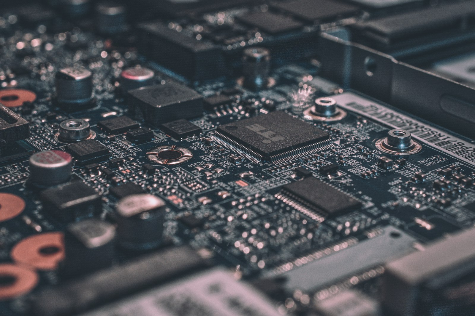
Artificial intelligence has triggered one of the largest industrial transformations in modern history. Behind every large language model, autonomous system, robotics platform, AI assistant, and hyperscale cloud deployment exists an immense semiconductor manufacturing ecosystem.
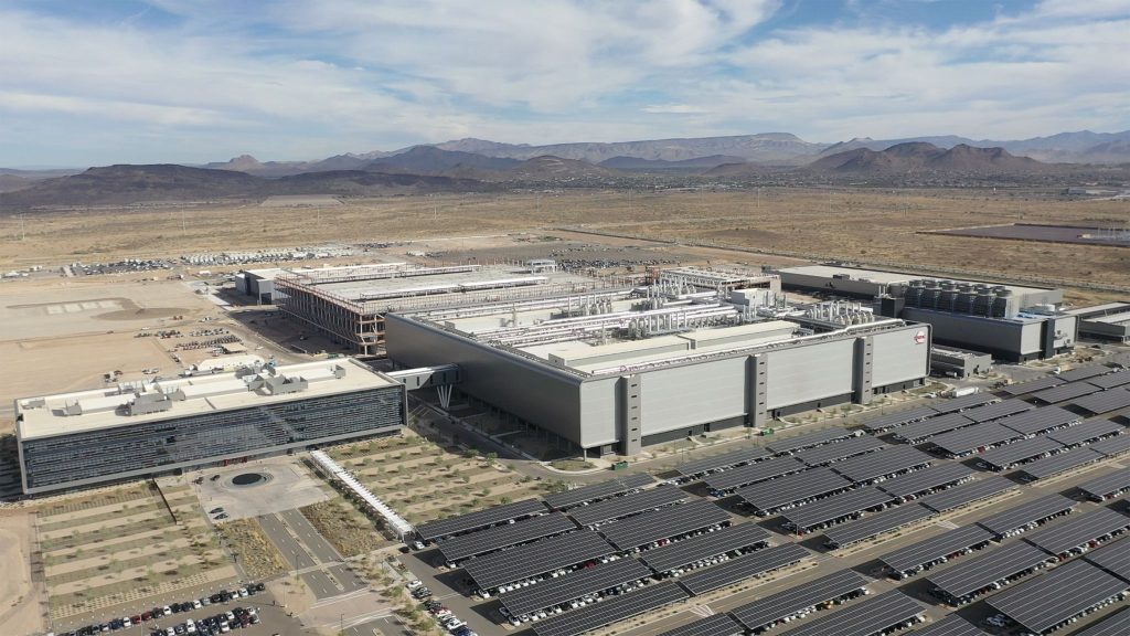
These advanced facilities are increasingly referred to as AI fabs. They combine semiconductor engineering, advanced materials science, robotics, nanometer-scale lithography, thermal engineering, packaging technology, and industrial-scale infrastructure.
Modern AI fabs are among the most technically sophisticated industrial environments ever built. They do not simply manufacture chips; they manufacture the computational foundation required for AI training, inference, automation, and next-generation digital infrastructure.
The Rise of AI Semiconductor Infrastructure
Traditional semiconductor fabs were originally optimized around CPUs, mobile processors, memory chips, and consumer electronics. Modern AI workloads have changed semiconductor priorities. The industry now requires massive parallel compute, extreme memory bandwidth, fast interconnects, low-latency packaging, and highly efficient power delivery.
Training large AI models requires enormous volumes of matrix multiplication. This is why GPUs, tensor processors, and custom AI accelerators have become so important. CPUs remain essential, but they are no longer the primary engine for large-scale AI training.
- Extreme parallel processing
- Massive memory bandwidth
- Ultra-fast interconnects
- Power-efficient tensor operations
- Advanced cooling infrastructure
- Specialized AI accelerators

Inside an AI Fab
An AI fab is not a single manufacturing line. It is a complete ecosystem of interconnected production stages involving design, wafer fabrication, packaging, testing, validation, deployment, and infrastructure integration.
The AI chip production chain begins with architecture and design. Engineers define the processor layout, memory interfaces, compute blocks, tensor engines, interconnect structure, and power delivery strategy. That design is then converted into masks and manufacturing instructions for the fab.
Wafer Fabrication Technology
Modern AI processors are manufactured on advanced silicon wafers using highly sophisticated lithography processes. A wafer may pass through hundreds or thousands of process steps before it becomes a finished semiconductor product.
The key stages include thin film deposition, lithography, etching, ion implantation, chemical mechanical planarization, metallization, cleaning, inspection, and electrical testing. Every stage must be controlled at extremely fine tolerances because tiny defects can reduce yield or destroy entire dies.
- Thin film deposition
- Extreme ultraviolet lithography
- Plasma etching
- Ion implantation
- Chemical mechanical planarization
- Metallization
- Inspection and metrology

EUV Lithography
Extreme Ultraviolet Lithography is central to modern AI chip production. EUV systems allow transistor features to be printed at nanometer scale using very short wavelength light. This enables dense transistor layouts required for high-performance AI accelerators.
EUV machines are extremely complex. They use plasma-generated light, reflective optics, vacuum chambers, precision masks, and nanometer-level alignment systems. The engineering difficulty is enormous, but EUV is essential for leading-edge nodes such as 5nm, 4nm, 3nm, and future 2nm-class processes.
HBM and AI Memory Systems
AI accelerators require extraordinary memory bandwidth. High Bandwidth Memory stacks are therefore integrated directly beside AI compute dies using advanced packaging systems. This allows the processor to move data between compute and memory far faster than traditional memory layouts.
HBM is critical because AI models are memory hungry. Large models require rapid access to weights, activations, embeddings, and intermediate tensor data. If memory cannot keep up, expensive compute units sit idle.

Advanced Packaging
Packaging has become one of the most important battlegrounds in AI semiconductor production. Traditional packaging is not enough for modern AI accelerators because the compute die must communicate with memory and other dies at extremely high speed.
Advanced packaging technologies allow multiple dies to behave almost like one integrated processor. This includes chiplet architectures, silicon interposers, 2.5D packaging, 3D stacking, wafer-level packaging, and hybrid bonding.
- CoWoS-style chip-on-wafer-on-substrate packaging
- 2.5D silicon interposer systems
- 3D die stacking
- Hybrid bonding
- Chiplet-based AI accelerators
- Wafer-level packaging
Tensor Processing Units
Tensor processing architectures are optimized specifically for neural network workloads. These systems accelerate matrix multiplication and tensor operations at enormous scale. Modern AI accelerators increasingly include tensor cores, systolic arrays, mixed precision engines, and specialized data movement units.
The key idea is simple: AI workloads repeatedly multiply and accumulate large matrices. Tensor hardware performs these operations far more efficiently than a general-purpose CPU. This is why tensor processors dominate AI training and inference.

AI Power and Cooling Infrastructure
Modern AI systems consume enormous electrical power. Large AI clusters may require megawatts of sustained power delivery. This creates major engineering challenges around voltage regulation, power conversion, heat removal, reliability, and monitoring.
Cooling is now a strategic design issue. Air cooling is reaching its limits for high-density AI systems. Many deployments increasingly use direct liquid cooling, cold plates, rear-door heat exchangers, and high-capacity coolant distribution units.

Testing, Yield and Binning
AI chips are extremely large and complex, so yield management is critical. A single wafer may contain many large dies, and any microscopic defect can reduce the number of usable processors. Manufacturers use inspection, metrology, wafer probing, burn-in testing, and binning to classify chips by performance and power characteristics.
Binning matters because not every chip performs identically. Some chips can run at higher clock speeds, lower voltage, or better thermal efficiency. These higher-performing parts are often reserved for premium products or enterprise AI systems.
The Future of AI Fabs
The next generation of AI fabs will likely involve even more advanced manufacturing technologies including sub-2nm process nodes, optical interconnects, wafer-scale AI processors, advanced 3D stacking, and hybrid bonding.
AI manufacturing is rapidly becoming one of the defining industrial sectors of the 21st century. The future of artificial intelligence may depend as much on manufacturing capability as it does on algorithms and software engineering.
- Sub-2nm process nodes
- Photonic computing
- Optical interconnects
- Wafer-scale AI processors
- Advanced 3D transistor structures
- Hybrid quantum-AI systems
- AI-optimized silicon materials